What the example programs do:
Example programs described here toggle PIO3_2 pin of the MCU 10 times a second. PIO3_2 is located at pin 43 or M43 on the PCB. First example is provided in assembly language and the second in C.
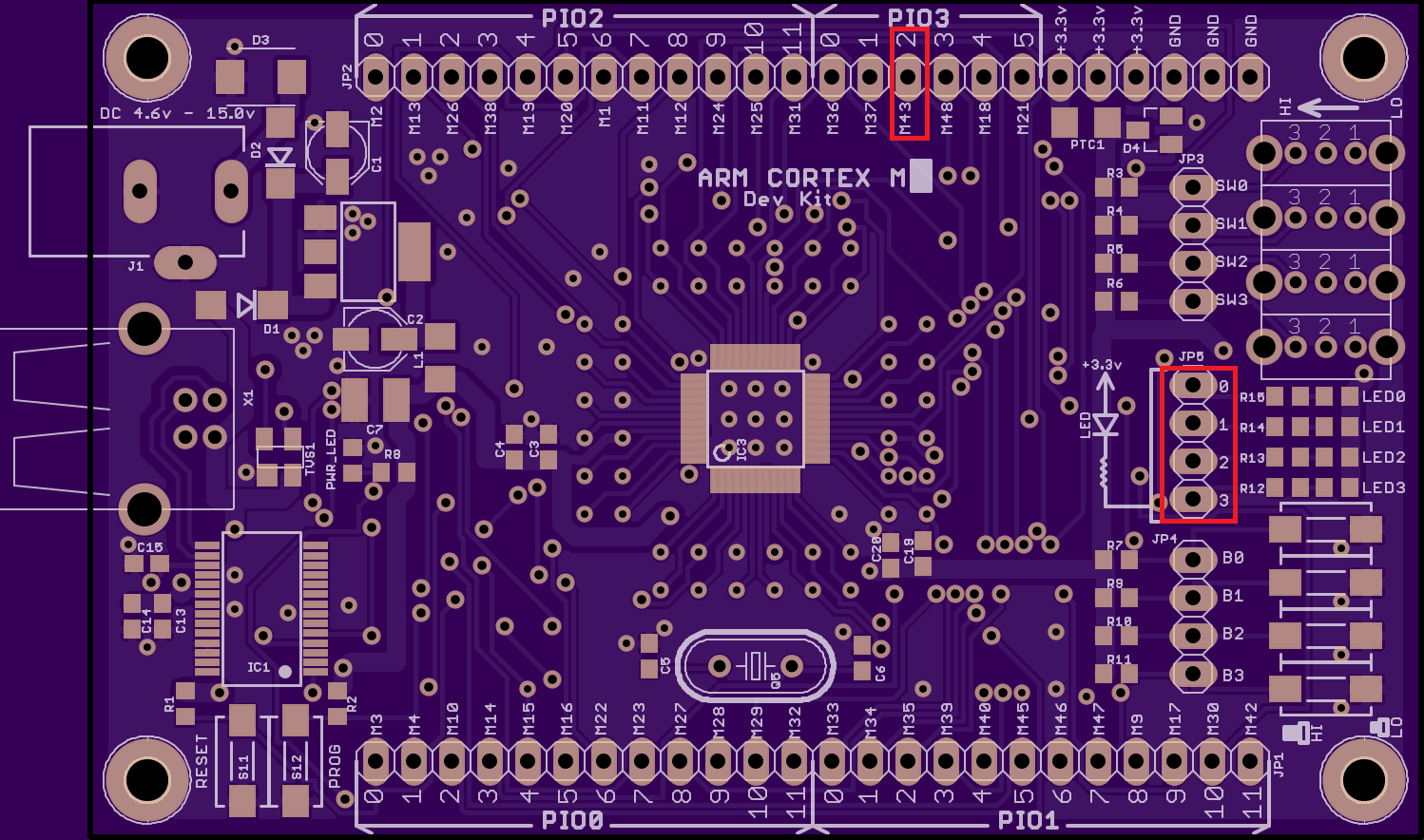 |
| Figure 1 |
Connect a wire between PIO3_2 and any pin of JP5 connector (red rectangle). This will allow the corresponding LED of JP5 to blink at 5Hz.
Development Environment Setup:
Development Environment Setup:
Keil project setup for assembly: Writing Assembly Code for ARM Cortex M0 (Device NXP LPC1114/301)
Keil Project setup for C: Writing C on ARM Cortex M0 (NXP LPC1114/301)
Program Flow:
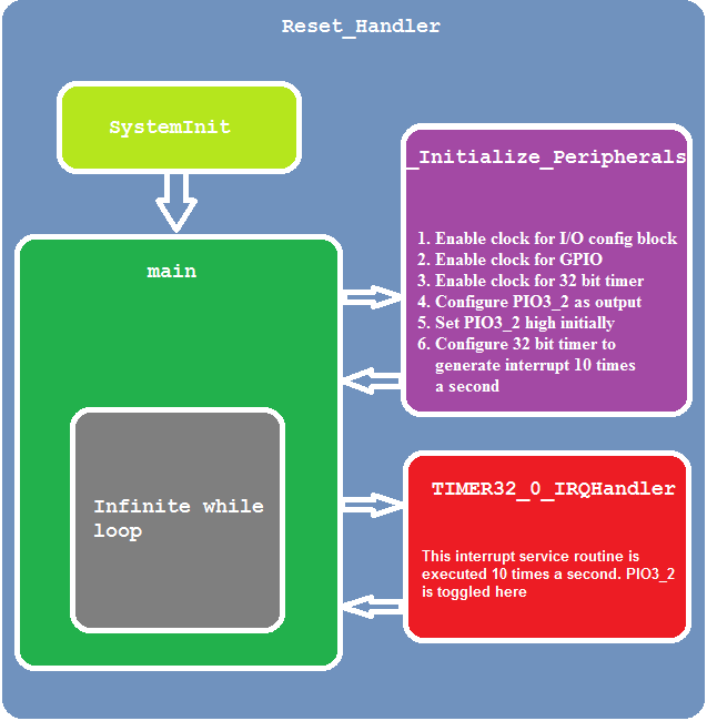 |
| Figure 2 |
On powerup or reset, Reset_Handler is executed first. Reset_Handler in starup_LPC11xx.s first invokes SystemInit routine before calling the __main routine. Keil usually copies the starup_LPC11xx.s file into the project directory when the project is created.
SystemInit routine configures the system PLL and clocks the MCU core with 48MHz. For C projects, SystemInit routine is defined in startup_LPC11xx.c. An assembly version of the SystemInit routine is provided in this example.
On completion of SystemInit routine, execution starts in __main. _Initialize_Peripherals routine is executed next in which following tasks are performed:
Task 1. Clock is enabled for the I/O configuration block
Task 2. Clock is enabled for the GPIO
Task 3. Clock is enabled for a 32-bit timer
Task 4. PIO3_2 (M43 on the PCB) is set as output. On reset, all the GPIO pins are configured as inputs by default.
Task 5. PIO3_2 is set (logic 1) initially
Task 6. 32-bit timer is configured so that it generates an interrupt 10 times a seconds (thus the 5Hz blink rate)
Program execution continues in __main after _Initialize_Peripherals routine returns. Global interrupts are enabled next. An infinite loop is executed in which some general calculations are performed.
Once the 32-bit timer-0 has counted 4.8 million CPU cycles, an interrupt request is generated and the interrupt service routine (ISR) TIMER32_0_IRQHandler is executed. The timer is configured in such a way that the count-value is reset at the time the counter has counted 4.8 million CPU cycles. PIO3_2 output is toggled in TIMER32_0_IRQHandler.
Example assembly code:
AREA main, CODE, READONLY
EXPORT __main
EXPORT __use_two_region_memory
__use_two_region_memory EQU 0
EXPORT SystemInit
EXPORT TIMER32_0_IRQHandler
ENTRY
; System Init routine
SystemInit PROC
; Initialize system clock to 48MHz from a 12MHz onboard crystal oscillator (XTAL)
; Description of the steps:
; Step 1: Power up system oscillator (XTAL)
; Step 2: Wait 200 counts in a while loop
; Step 3: Select system oscillator (XTAL) as the input of the PLL clock source
; Step 4: Wait until PLL clock source is updated to 12MHz system oscillator (XTAL)
; Step 5: Set the clock multiplier for the PLL and power up the System PLL
; Step 6: Wait until PLL is locked
; Step 7: Select the output of the PLL as the main CPU clock
; Step 8: Toggle the main CPU clock enable bit for the
; new clock source (PLL output) to take effect
; Step 9: Wait until main CPU clock is updated
; Step 10: Set the core and peripheral clock divider to 1
; Step 1: Power up system oscillator (XTAL)
; Load the address of PDRUNCFG into R0;
LDR R0, =(0x40048238); PDRUNCFG, address 0x4004 8238
; Load the value of PDRUNCFG into R1
LDR R1, [R0];
; Clear SYSOSC_PD(bit 5) in PDRUNCFG
LDR R2, =(0xFFFFFFDF);
ANDS R1, R2;
; Store the R2 into PDRUNCFG
STR R1, [R0];
; Step 2: Wait 200 counts in a while loop
MOVS R0, #(0xC7);
MOVS R1, #(0x01);
_WAIT_OSCILLATOR_PWR_UP
SUBS R0, R1;
BNE _WAIT_OSCILLATOR_PWR_UP; Loop until ZERO flag is 1
; Step 3: Select system oscillator (XTAL) as the input of the PLL clock source
LDR R0, =(0x40048040); SYSPLLCLKSEL, address 0x4004 8040
; Load R1 with 0x01 to select the system oscillator for the PLL
MOVS R1, #(0x01);
; Store the value of R1 into SYSPLLCLKSEL
STR R1, [R0];
; Toggle enable bit for the change to take effect in SYSPLLCLKUEN, address 0x4004 8044
; (System PLL clock source update enable register) to update PLL clock source
LDR R0, =(0x40048044); SYSPLLCLKUEN, address 0x4004 8044
MOVS R1, #(0x01);
MOVS R2, #(0x00);
; Write 1 to SYSPLLCLKUEN
STR R1, [R0];
; Write 0 to SYSPLLCLKUEN
STR R2, [R0];
; Write 1 again to SYSPLLCLKUEN
STR R1, [R0];
; Step 4: Wait until PLL clock source is updated to 12 MHz system oscillator (XTAL)
; Load the address of SYSPLLCLKUEN into R0
LDR R0, =(0x40048044); SYSPLLCLKUEN, address 0x4004 8044
MOVS R2, #(0x01); Value to check against in the following loop
_WAIT_PLL_CLK_SRC_UPDATE
; Load the value of SYSPLLCLKUEN into R1
LDR R1, [R0];
CMP R1, R2;
BNE _WAIT_PLL_CLK_SRC_UPDATE; Loop until PLL clock source is updated
; Step 5: Set the clock multiplier for the PLL and power up the System PLL
; Load the address of SYSPLLCTRL
LDR R0, =(0x40048008); SYSPLLCTRL, address 0x4004 8008
; Load R1 with the MSEL and PSEL values to render 48MHz from 12MHz system oscillator
MOVS R1, #(0x23);
; Store R1 into SYSPLLCTRL
STR R1, [R0];
; Power up System PLL = Clear bit 7 of PDRUNCFG
; Load the address of PDRUNCFG into R0;
LDR R0, =(0x40048238); PDRUNCFG, address 0x4004 8238
; Load R1 with PDRUNCFG
LDR R1, [R0];
; Load R2 with 0xFFFFFF7F (only bit 7 is cleared)
LDR R2, =(~(1<<7));
; And the values of R1 (which is PDRUNCFG) and R2
ANDS R1, R2;
; Store the new value of R1 into PDRUNCFG
STR R1, [R0];
; Step 6: Wait until PLL is locked
; Load the address of SYSPLLSTAT into R0
LDR R0, =(0x4004800C); SYSPLLSTAT, address 0x4004 800C
; Load the value of PLL lock status to check against in to R2
MOVS R2, #(0x01);
_WAIT_UNTIL_PLL_LOCKED
; Load SYSPLLSTAT into R1
LDR R1, [R0];
; Check against PLL lock status bit pattern saved in R2
CMP R1, R2;
BNE _WAIT_UNTIL_PLL_LOCKED; Loop until PLL is locked
; Power up the watch dog timer clock here if required
; Step 7: Select the output of the PLL as the main CPU clock
; Load the address of MAINCLKSEL in to R0
LDR R0, =(0x40048070); MAINCLKSEL, address 0x4004 8070
; Load R1 with 0x03 (0x03 = PLL output as the main CPU clock)
MOVS R1, #(0x03);
; Store the value of R1 into MAINCLKSEL
STR R1, [R0];
; Step 8: Toggle the main CPU clock enable bit for the
; new clock source (PLL output) to take effect
; Load the address of MAINCLKUEN into R0
LDR R0, =(0x40048074); MAINCLKUEN, address 0x4004 8074
; Load 0x01 into R1
MOVS R1, #(0x01);
; Load 0x00 into R2
MOVS R2, #(0x00);
; Enable MAINCLKUEN
STR R1, [R0];
; Disable MAINCLKUEN
STR R2, [R0];
; Enable MAINCLKUEN
STR R1, [R0];
; Step 9: Wait until main CPU clock is updated
; Load the address of MAINCLKUEN into R0
LDR R0, =(0x40048074); MAINCLKUEN, address 0x4004 8074
; Load 0x01 into R2
MOVS R2, #(0x01);
_WAIT_MAIN_CLK_UPDATE
; Load the value of MAINCLKUEN into R1
LDR R1, [R0];
; Compare if MAINCLKUEN(R1) is updated or not
CMP R1, R2;
BNE _WAIT_MAIN_CLK_UPDATE; Loop until main CPU clock source is updated
; Step 10: Set the core and peripheral clock divider to 1
; Load the address of SYSAHBCLKDIV into R0
LDR R0, =(0x40048078); SYSAHBCLKDIV, address 0x4004 8078
; Load 0x01 into R1
MOVS R1, #(0x01);
; Store 0x01 into SYSAHBCLKDIV
STR R1, [R0];
BX LR; Return from SystemInit
ENDP; End of SystemInit routine
_Initialize_Peripherals PROC
PUSH {LR}; Other registers can be pushed to the stack if necessary
; Enable clock for I/O config block, GPIO, and 32-bit counter/timer in SYSAHBCLKCTRL
; First, load the address of SYSAHBCLKCTRL into R0
LDR R0, =(0x40048080); SYSAHBCLKCTRL, address 0x4004 8080
; Load R1 with the value of SYSAHBCLKCTRL
LDR R1, [R0];
; Load the bit pattern to enable clock for I/O config block(bit 16), GPIO(bit 6),
; and 32-bit counter/timer(bit 9) into R2
LDR R2, =( (1<<16) | (1<<9) | (1<<6) );
; Apply bitwise OR between R1(value of SYSAHBCLKCTRL) and R2(new bit pattern)
; and save the result into R1
ORRS R1, R2;
; Store the new value of R1 into SYSAHBCLKCTRL
STR R1, [R0];
; Configure PIO3_2 (pin 43, M43 on PCB) as output
; By default (on reset), all the GPIO pins are inputs
; Set bits 2:0 of IOCON_PIO3_2 to zeros for PIO3_2 function (not the DCD function)
; Load the address of IOCON_PIO3_2 into R0
LDR R0, =(0x4004409C); IOCON_PIO3_2, address 0x4004 409C
; Load the value of IOCON_PIO3_2 into R1
LDR R1, [R0];
; Load R2 with 0xFFFFFFF8 (bits 2:0 are zeros)
LDR R2, =(0xFFFFFFF8);
; Apply AND operation between R1 and R2
ANDS R1, R2;
; Store the new value of R1 into IOCON_PIO3_2
STR R1, [R0];
; Set bit 2 of GPIO3 data direction register to set PIO3_2 pin as output
; Load the address of GPIO3DIR into R0
LDR R0, =(0x50038000); GPIO3DIR, address 0x5003 8000
; Load the value of GPIO3DIR into R1
LDR R1, [R0];
; Load a bit pattern 0x00000004 into R2 (bit 2 is set)
MOVS R2, #( (1<<2) );
; Apply bitwise OR operation between R1(value of GPIO3DIR) and R2(bit pattern)
ORRS R1, R2;
; Store the new value of R1 into GPIO3DIR;
STR R1, [R0];
; Set the initial output on PIO3_2(M43) as high
; Load the address of GPIO3DATA(last unmasked address base+0x3FFC) into R0
LDR R0, =(0x50033FFC); GPIO3DATA Base + 0x3FFC, address 0x5003 3FFC
; Load the value (1) at bit location 2 to set PIO3_2 high
MOVS R1, #( (1<<2) );
; Store the value of R1 into GPIO3DATA
STR R1, [R0];
; Initialize 32-bit Counter/Timer0 such that it generates
; an interrupt 10 times a second (= 5 ONs + 5 OFFs = 10Hz timer)
; Load Match Register0(TMR32B0MR0) of 32-bit counter0(TMR32B0 or CT32B0)
; with (48MHz/10Hz - 1) = (4800000-1) = 4799999
LDR R0, =(0x40014018); TMR32B0MR0, address 0x4001 4018
LDR R1, =(0x00493DFF); Decimal 4799999 = Hexadecimal 0x00493DFF;
; Store the value of R1 into TMR32B0MR0
STR R1, [R0];
; Enable interrupt when the value in the counter(TMR32B0TC) matches
; the value in Match Register0 (TMR32B0MR0) and at the same time
; resets the 32-bit counter. Thus the counter starts to count from 0 again.
; Load the address of Match Control Register(TMR32B0MCR) into R0
LDR R0, =(0x40014014); TMR32B0MCR, address 0x4001 4014
; Load the value of TMR32B0MCR into R1
LDR R1, [R0];
; Enable Interrupt on MR0 and reset counter value on match (set bit 0 and bit 1 of TMR32B0MCR)
MOVS R2, #( (1<<1)|(1<<0) ); Load R2 with bit 0 and bit 1 set. All other bits are zeros
; Apply OR operation between R1(value of TMR32B0MCR) and R2
ORRS R1, R2;
; Store the new value of R1 into TMR32B0MCR
STR R1, [R0];
; Enable CT32B0 interrupt (bit 18) in Nested Vectored Interrupt Controller(NVIC)
; Load the address of Interrupt Set Register(ISER) of NVIC into R0
LDR R0, =(0xE000E100); ISER of NVIC, address 0xE000 E100
; Load R1 with all zeros except bit-18 set
LDR R1, =( (1<<18) ); "MOVS" can only load immediate values from 0 - 255 decimal
; Store the value of R1 into ISER of NVIC
STR R1, [R0];
; Start the counter by setting bit 0 of Timer Control Register(TCR)
LDR R0, =(0x40014004); TMR32B0TCR, address 0x4001 4004
; Load R1 with all zeros except bit 0 set
MOVS R1, #(0x01);
; Store R1 into TMR32B0TCR. This starts the counter
STR R1, [R0];
;Return from the function _Initialize_Peripherals
POP {PC};
ENDP; End of _Initialize_Peripherals
; Interrupt Service Routine (ISR) for TMR32B0.
; The name of the service routine is defined in startup_LPC11xx.s
TIMER32_0_IRQHandler PROC
; Save the register values onto the stack that will be used in this ISR
PUSH {R0, R1, R2};
; Toggle PIO3_2 (pin 43 or M43 on PCB)
; Load the address of GPIO3DATA(last unmasked address base+0x3FFC) into R0
LDR R0, =(0x50033FFC); GPIO3DATA Base + 0x3FFC, address 0x5003 3FFC
; Load the value of GPIO3DATA into R1
LDR R1, [R0];
; Load R2 with (1<<2)
MOVS R2, #(1<<2);
; Apply bitwise XOR between R1(the value of GPIO3DATA)
; and R2 (1<<2) to toggle the value of bit location 2
EORS R1, R1, R2;
; Store the new value of R1 into GPIO3DATA
STR R1, [R0];
; Clear interrupt by writing 1 to the MR0 interrupt(bit 0) of Interrupt Register(TMR32B0IR)
LDR R0, =(0x40014000); TMR32B0IR, address 0x4001 4000
MOVS R1, #(0x01);
STR R1, [R0];
; Get the registers back from the stack that were saved at the beginning of this ISR
POP {R0, R1, R2};
; Return from TIMER32_0_IRQHandler Interrupt Service Routine
BX LR;
ENDP; End of TIMER32_0_IRQHandler
; __main routine starts here
__main PROC
; Call the following function to initialize peripherals
BL _Initialize_Peripherals;
; Enable global interrupts
CPSIE i;
; Loop infinitely between "_LoopHere1" and "B _LoopHere1"
MOVS R0, #(0x00); Test load 1.
; "MOVS" can only load immediate values from 0 - 255 decimal
_LoopHere1
NOP;
NOP;
MOVS R1, #(0x02); Test load 2
; Increment R0 by 1
ADDS R0, R0, #(0x01); R0 = R0 + 1;
; Test 1 cycle 32-bit hardware multiplier
MULS R1, R0, R1; 1 cycle multiply operation R1 = R0 x R1
NOP;
NOP;
B _LoopHere1
NOP;
ENDP; End of __main
END; End of File
|
Example C code:
#include "LPC11xx.h"
void _Initialize_Peripherals(void)
{
volatile unsigned int tempData = 0;
// Enable clock for I/O config block, GPIO, and 32-bit counter/timer in SYSAHBCLKCTRL
// Load the bit pattern to enable clock for I/O config block(bit 16), GPIO(bit 6),
// and 32-bit counter/timer(bit 9) int SYSAHBCLKCTRL
LPC_SYSCON->SYSAHBCLKCTRL |= ( (1<<16) | (1<<9) | (1<<6) );
// Configure PIO3_2 (pin 43, M43 on PCB) as output
// By default (on reset), all the GPIO pins are inputs
// Set bits 2:0 of IOCON_PIO3_2 to zeros for PIO3_2 function (not the DCD function)
tempData = LPC_IOCON->PIO3_2;
tempData = tempData & 0xFFFFFFF8;
LPC_IOCON->PIO3_2 = tempData;
// Set bit 2 of GPIO3 data direction register to set PIO3_2 pin as output
LPC_GPIO3->DIR |= (1<<2);
// Set the initial output on PIO3_2(M43) as high
LPC_GPIO3->DATA |= (1<<2);
// Initialize 32-bit Counter/Timer0 such that it generates
// an interrupt 10 times a second (= 5 ONs + 5 OFFs = 10Hz timer)
// Load Match Register0(TMR32B0MR0) of 32-bit counter0(TMR32B0 or CT32B0)
// with (48MHz/10Hz - 1) = (4800000-1) = 4799999
LPC_TMR32B0->MR0 = 0x00493DFF; //Decimal 4799999 = Hexadecimal 0x00493DFF;
// Enable interrupt when the value in the counter(TMR32B0TC) matches
// the value in Match Register0 (TMR32B0MR0) and at the same time
// resets the 32-bit counter. Thus the counter starts to count from 0 again.
LPC_TMR32B0->MCR |= ( (1<<1)|(1<<0) );
// Enable CT32B0 interrupt (bit 18) in Nested Vectored Interrupt Controller(NVIC)
NVIC_EnableIRQ(TIMER_32_0_IRQn); // "TIMER_32_0_IRQn" is defined in LPC11xx.h
// Start the counter by setting bit 0 of Timer Control Register(TCR)
LPC_TMR32B0->TCR = (1<<0);
} // End of _Initialize_Peripherals
// Interrupt Service Routine (ISR) for TMR32B0.
// The name of the service routine is defined in startup_LPC11xx.s
__irq void TIMER32_0_IRQHandler(void)
{
// Toggle PIO3_2 (pin 43 or M43 on PCB)
// Apply bitwise XOR between GPIO3DATA and 1 in bit location 2 (1<<2)
LPC_GPIO3->DATA = ( LPC_GPIO3->DATA ^ (1<<2) );
// Clear interrupt by writing 1 to the MR0 interrupt(bit 0) of Interrupt Register(TMR32B0IR)
LPC_TMR32B0->IR = (1<<0);
} // End of TIMER32_0_IRQHandler
void __main(void)
{
// SystemInit() routine is executed before __main()
// SystemInit() routine is defined in system_LPC11xx.c
// system_LPC11xx.c is located at "keil_installation\ARM\Startup\NXP\LPC11xx"
volatile unsigned int tempData0;
volatile unsigned int tempData1;
// Call the following function to initialize peripherals
_Initialize_Peripherals();
// Enable global interrupts
__enable_irq();
// Infinite while loop
while(1)
{
__NOP();
__NOP();
tempData1 = 2;
// Increment tempData0 by 1
tempData0++;
tempData1 = tempData0 * tempData1; // Multiply operation
__NOP();
__NOP();
} // end of while(1)
} // End of __main
|
Instruction are provided here (step 8 to step 10) to compile, simulate and run the above programs on the development kit.
No comments:
Post a Comment